Bolometers
The bolometer key parameters are the thermal resistance and the heat capacity. As is shown in Section 3.2, the low- frequency voltage responsiv- ity, of the thermal detector (ш « l/r№, where rth is the thermal response time) is proportional to the thermal resistance, Rth, and does not depend on the heat capacitance. At the opposite side, for high frequencies (w » l/r(/l), the voltage responsivity is not dependent on Rth but is inversely proportional to the heat capacitance.
From considerations presented in Chapter 3, the thermal conductance from the detector to the outside world should be small (i.e., the thermal resistance should be high). The smallest possible thermal conductance would occur when the detector is completely isolated from the environment under vacuum, with only radiative heat exchange between it and its heat-sink enclosure.
It was discovered that graphene assumes a low volume for a given area and a low density of states, resulting in a low heat capacity, and exhibiting
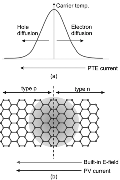
FIGURE 6.8 Photocurrent generation in a graphene p-n junction: (a) profile of carrier concentrations due to light intensity distribution, (b) built-in electric field of p-n junction as well as PTE effect leading to photovoltaic current flow from n-type to p-type region (adapted after Ref [10]).
a fast device response. The electron cooling by acoustic phonons is unproductive (owing to the small Fermi surface) and cooling by optical phonons requires a high temperature (kT> 200 meV), leading to the fact that thermal resistance is relatively high, giving rise to bolometric sensitivity [3,11].
Graphene is characterized by over 100-fold anisotropy of heat flow between the in-plane and out-of-plane directions [12]. High in-plane thermal conductivity is due to covalent sp2 bonding between carbon atoms, whereas out-of-plane heat flow is limited by weak van der Waals coupling. The in-plane thermal conductivity of graphene at room temperature is among the highest of any known material, about 2000-4000 W/mK for a freely suspended sample (Fig. 6.9) [12]. The heat flow perpendicular to the graphene sheet is limited with adjacent substrates, e.g. Si02. It is interesting that the thermal resistance between graphene and its environment dominates that between individual graphene sheets. The discovery

FIGURE 6.9 Room-temperature ranges of thermal conductivity for diamond, graphite, carbon nanotubes (CNTs), graphene, and graphene nanoribbons (GNRs) (after Ref [12]).
of graphene was quickly followed by many other such materials, including MoS2, bP, and hBN, etc.
There are some technical challenges in fabrication of 2D-material bolometers. In graphene, with weak electron-phonon scattering, the resistance is weakly temperature dependent [11]. In consequence, it is challenging to measure the electron temperature change due to incoming radiation power. In addition, to achieve the small electron-phonon thermal conductance, strong thermal isolation is required, which is difficult to achieve. In the case of terahertz detectors, low impedance is required to match the antenna to the external readout circuit, which is also challenging.
2D materials are naturally great candidates for nano electromechanical systems (NEMS) applications. Graphene can sustain large elastic deformations due to its extreme flexibility and could have a positive effect on the device’s dynamic range.
Field-Effect Transistor Detectors
Nonlinear properties of plasma wave excitations (the electron density waves) in nanoscale field-effect transistor (FET) channels enable their response at frequencies appreciably higher than the device cutoff frequency, which is due to electron ballistic transport. In the ballistic regime of operation, the momentum relaxation time is longer than the electron transit time. The FETs can be used either for resonant (tuned to a certain wavelength) or non-resonant (broadband) THz detection and can be directly tunable by changing the gate voltage.
The graphene FET can also be used for detection of TFIz radiation, which was first proposed by Dyakonov and Shur in 1993, based on a formal analogy between the equations of the electron transport in a gated 2D transistor channel and those describing the shallow water behavior or acoustic waves in musical instruments, indicating that the hydrodynamiclike effect should exist also in the carrier dynamics in the channel [13]. It must be stressed that instability of that flow in the form of plasma waves was predicted under certain boundary conditions.
The physical mechanism supporting the development of stable oscillations lies in the reflection of plasma waves at the borders of a transistor, with subsequent amplification of the wave’s amplitude. Plasma excitations in FETs with sufficiently high electron mobility can be used for emission as well as detection of THz radiation [14,15].
The plasma waves in FETs are characterized by the linear dispersion law [13], and in a gated region:

where s is the plasma wave velocity in the channel, is the gate voltage, Vlh is the threshold voltage, к is the wave vector, q is the electron charge, and m* is the electron effective mass.
The plasma wave velocity in the gated region tends to be noticeably larger than the electron drift velocity. A short FET channel, with length Lg, acts as a resonant cavity for these waves with the eigenfrequencies a>„ = a>0(l + 2n) (n = 1,2,3,...). The fundamental plasma frequency is

When Wgi « 1, where т is the momentum relaxation time, the detector response is a smooth function of ш and (broadband detector). When ш0г » 1, the FET can operate as a resonant detector, tunable by the gate voltage response frequency, and this device can operate in the THz range. The detection character (resonant or nonresonant) depends on the quality factor of the transistor resonating cavity.
Assuming m* « 0.1mo (m0 is the free electron mass), Lg « 100 nm, and V, the frequency of plasma waves is estimated to be v0 = wJ2n « 3 THz. The minimum gate length can approach « 30 nm, and, thus, v0 can reach 12-14 THz for FETs with GaAs channels.
Summarizing the above discussion, the detection by FETs is due to nonlinear properties of the transistor, leading to the rectification of the AC current induced by the radiation, where photoresponse appears in the form of a DC voltage between the source and the drain, and is proportional to the radiation intensity (PV effect). In the resonant regime, the plasma waves are dimly damped (when a plasma wave launched at the source can reach the drain in a time shorter than the momentum relaxation time) and the detection mechanism exploits interference of the plasma waves in the cavity, resulting in a resonantly enhanced response. Figure 6.10 schematically shows the resonant oscillation of plasma waves in FET’s gated region. Even if there is no extra antenna in the system, the THz radiation is coupled to the FET by contact pads and bonding wires. An improvement in sensitivity can be reached by adding a proper antenna or a cavity coupling. Broadband detection occurs when plasma waves are overdamped (meaning that the plasma waves launched at the source decay before they reach the drain).
The photovoltage dependence on carrier density in the FET channel also shows PTE contributions. Figure 6.11 presents and schematically explains two competitive independent detection effects: the plasmonic

FIGURE 6.10 (a) THz CMOS detector and (b) plasma oscillations in a transistor.

FIGURE 6.11 The detection mechanism in graphene FET THz photodetector.
detection effect due to the nonlinearity of electron transport, and the thermoelectric effect due to the presence of both carrier density junctions and the induced temperature gradient across the FET channel. The red region indicates the locally heated area at the interface of ungated and gated sections with thermopowers Sug and Sg, respectively. Even though strongly counterbalanced by the thermoelectric response, the plasma wave detection is the dominant mechanism.

