Terahertz Detectors
Diverse optoelectronic properties of 2D materials cover a wide range of the electromagnetic spectrum. Recently, efforts have increased to also develop the proof-of-concept for THz photodetectors. The finite and direct bandgap in both the bulk (Eg « 0.35 eV) and monolayer bP (Eg « 2 eV) phase, and its considerably greater mobility (>1000 cm2/Vs), make it a good trade-off between graphene and TMDs. Furthermore, the achievable on-off transistor ratio greater than 105 makes bP a suitable candidate for detection of THz-frequency light.
In 2015, Viti et al. first demonstrated that bP THz photodetectors operated at room temperature [29]. They exploited the integration of a mechanically Si02-encapsulated bP flake in an antenna-coupled top-gate FET, as is shown in Fig. 7.8. A standard adhesive tape technique was used to transfer the flake onto a 300-nm thick Si02 layer on the top of a 300- |tm intrinsic silicon wafer. The selected bP flakes, with thickness of about 10 nm, coincide with the out-of-plane screening length and correspond to »16 layers of phosphorene. This choice ensures an ideal compromise between high mobility and large carrier density tunability.

FIGURE 7.8 Vertical sketch of the ЬР-FET structure.

FIGURE 7.9 Fabrication of the ЬР-FET structure: (a) design of the device [the channel length (Lc) is 2.7 pm and the gate length {Lg) is 530 nm], (b) S and G electrodes are designed to form а 500-pm, 90° flare angle, planar bow-tie, antenna; the D electrode is connected to a rectangular bonding pad.
THz FET detectors have been fabricated by exploiting a combination of electron-beam lithography and metal evaporation. The source (S) and gate (G) electrodes were patterned in the shape of two halves of a planar bow-tie antenna, having a total length 2L = 500 pm, and a flare angle of 90°, in resonance with the 0.3 THz radiation. Figure 7.9 shows the device layout [29].
The photodetection mechanism in bP-based THz FETs was identified as a consequence of three mechanisms, including photothermoelectric, bolometric, and plasma-wave rectification effects [29], and the anisotropy of bP [30]. For example, Fig. 7.10 shows the extrapolated NEP curves for the above three mechanisms, the minimum of which reaches 7 nW/HzI/2, 10 nW/Hz1/2, and 45 nW/HzI/2 for the bP-bolometer, plasma-wave, and thermoelectric detector, respectively. The responsivity value of ~5-8 A/W at about 0.3 THz permits the use of the bP FET device in application for real-time pharmaceutical and quality control imaging [30].

FIGURE 7.10 Noise equivalent power as a function of gate voltage (Vg) for the plasma-wave sample (0.29 THz), thermoelectric sample (0.32 THz) and bolomet- ric sample detectors (after Ref. [30]).

FIGURE 7.11 hBN/bP/hBN heterostructure THz FET detectors: (a) AFM tomographic image of the top-gate FET, (b) optical microscopy image of the fabricated device. The bow arm length is L = 250 pm (after Ref. [31]).
To prevent fast degradation of the exfoliated bP flake at ambient temperature, Viti et al. embedded a bP flake within a natural semiconductor heterostructure, formed by multilayered h-BN crystals, to devise hBN/bP/ hBN heterostructure THz FET detectors, as shown in Fig. 7.11. The heterostructure was fabricated as previously (see Fig. 7.8) over a high-resistivity silicon substrate covered with a Si02 cap layer. A 40-nm thick hBN flake with lateral dimensions 20x20 pm2 was put on the Si02/Si substrate to facilitate the subsequent alignment step, transferring the bP flake onto the lower hBN layer. Before the deposition of the hBN top layer, the source (S) and drain (D) contacts were defined through a combination of electron- beam lithography and metal deposition on the bP flake.
The FET hBN/bP/hBN heterostructure, operating at 295 GFIz, is characterized by a minimum NEP of 100 pW/FIz1/2 and maximum Rv = 38 V/W at 4 K, whereas, at room temperature, the corresponding values are ~ 10 nW/Hz1/2 and ~2 V/W, respectively. hBN as an atomic dielectric constitutes a good encapsulating material for bP. In addition, hBN is a valuable gate dielectric, which, in turn, allows high gate-to-channel capacitance for tuning the device transport and optical properties. Viti et al. [32] reviewed recent research on bP detectors operating in a wider spectral range, from 0.26 THz to 3.4 TPIz, with emphasis on the future challenges in the fabrication of stable and reliable optical and electronic technologies.
Recently, it was demonstrated that topological insulators can also be promising candidate materials for broadband photodetection, including the THz range. Topological insulators (TIs) represent a novel quantum phase of matter, characterized by a semiconducting bulk and topologically protected surface states, with spin and momentum helical locking and a Dirac-like band structure [33,34]. 2D TIs are associated with gapless edge states, and three-dimensional (3D) insulators with gapless topological surface states (TSS) [35].
Intriguing properties of TIs result from:
- • The gapless state of TSS, which enable carrier generation by light absorption over a very wide energy spectrum, including the THz range,
- • Optoelectronic properties, which can be engineered by material stoichiometry [36],
- • High TSS mobility, even higher than that of graphene, due to the topological protection that prevents back-scattering effects [37], and
- • 2D TSS electron gas of 3D TIs supports a collective excitation (Dirac plasmons) in the THz range [38].
Most of the published papers concern visible and short-wavelength infrared TIs photodetectors [39]. The promising application of THz plasmonics with TIs is related to the rectification of THz radiation via the excitation of plasma waves in the active channel of antenna-coupled FETs.
The first demonstration of THz detection, mediated by TSS in top-gated nanometer FETs, exploiting thin Bi2Te,_xSex flakes, was demonstrated by
Viti et al. in 2016 [40] (Fig. 7.12). Flakes having a total length < 2 pm have been selected as active nonlinear elements of FETs, in order to reduce both the parasitic capacitance and the resistances in the ungated transistor regions. By engineering the Bi2Te3_xSex stoichiometry, and mediating the room temperature THz detection with overdamped plasma-wave oscillations, a maximum responsivity of 3.0 V/W, and a minimum NEP of ~10 nW/Hz1/2 have been achieved for a 292.7-GHz impinging radiation frequency. Using this detector, the 400 X 700 pixel image of a target object was acquired with a time constant of 20 ms. This experiment gives a realistic account of the exploitation of TSS for large-area, fast THz imaging.
Another structure of TI THz photodetectors has also been proposed. Yao et al. [41] proposed a Bi2Te3-Si heterojunction detector, schematically shown in Fig. 7.13(a). The Bi2Te, film, 300-pm in diameter and 100-nm in thickness, was grown onto the Si wafer by pulsed laser deposition. Pt and Ag electrode contacts were then deposited on the top surface of the Bi2Te3 and the bottom surface of the Si, respectively. The device demonstrated photoresponse at room temperature in the wavelength range from the ultraviolet (370.6 nm) to terahertz (118 pm).
An innovative strategy for the direct detection of THz photons at room temperature, based on a subwavelength metal- Bi2Se3-metal structure, has been proposed in Ref. [42] [Fig. 7.13(b)]. In this device, the contact metal converts incident radiation into a localized surface-plasmon field, which drives the TSS back and forth. The measured room-temperature responsivity of the device, working in the self-powered and bias modes at
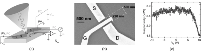
FIGURE 7.12 Top-gated nanometer FET exploiting a thin Bi2Te3_xSex flake: (a) schematics of the THz detection principle, where photovoltage and photocurrent modes are depicted in black and purple, respectively; (b) false-color SEM image of the top-gated FET; S, G, and D stand for source, gate, and drain, respectively; and (c) experimental responsivity measured at room temperature at a fixed frequency I/ = 292.7 GHz, while sweeping the gate-bias Vg in the range (-10 V, + 10 V) (after Ref. [40]).

FIGURE 7.13 Structures of THz photodetectors with topological insulators: (a) Bi2Te3-Si heterojunction in a two-pole structure (the forward bias is defined as applying a positive bias on the Bi2Te3 side), (b) metal-Bi2Se3-metal structure (the spacing distance L between the two gold contacts is much shorter than the wavelength radiation).
0.3 THz, was 75 and 475 A/W, respectively. The NEP value of 3.6 X lCk13 W/Hzl/2 and the detectivity of 2.17 X 10¹¹ cmHz1/2/W was achieved for a device working under a bias current of 50 mV. These results are crucial for the successful use of TIs in the field of THz imaging applications.

