Thermal Stresses in a Flip-Chip Design
“The truth is rarely pure and never simple."
—Oscar Wilde, Irish dramatist and novelist
Background/Incentive
Flip-chip (FC) technology (Figure 7.1), suggested about 50 years ago by the General Electric Light Military Electronics Dept, in Utica, New York, rapidly became widespread in the electronic industry owing to its ability to minimize the real estate occupied by an IC package. FC solder joints provide, in addition to electrical connection, mechanical support for the chips. This makes FC designs prone to physical failures. Various measures, including “dummy” solder joints (i.e., joints not needed to provide electrical connections) were suggested over the years to improve the situation. Particularly, a variety of encapsulation (“underfill”) technologies were investigated and applied. It has been established that FC and fine-pitch ball-grid array (FPBGA) package designs are an attractive way to pursue as far as small-size and low-cost of IC packages are concerned. There are, however, situations when the acceptable reliability level in FC and FPBGA technologies cannot be achieved without bringing in surrogate materials, s.c. underfills, between the chip and its substrate to strengthen the solder joint interconnections. Underfill technology was suggested, among other possible encapsulation technologies, about three decades ago [1], but has become the technology of choice in today’s IC packaging. Solder material fatigue failures caused by the inelastic thermal strains in the peripheral portions of the solder joint interconnections and delaminations (typically at the chip-solder interface) were observed and established as the main failure modes in FC and FPBGA structures with underfills. It is nonetheless expected that the appropriately chosen underfill material and the adequate application technology will improve the situation. Of course, one should determine, first of all, if it would be possible to get away with an unencapsulated design (“to underfill or not to underfill: that’s the question?”) and still meet the reliability requirements. If, however, an underfill decision is made, one should select the adequate underfill material and technology, with consideration of numerous factors associated with the application of this technology: encapsulation process, time- to-market (completion), cost, manufacturability, testability, reparability, and so on. The published experimental and modeling work on the mechanical performance and reliability of FC designs is enormous (see, for example, [1-31]). As to the modeling work, it was conducted by mostly using finite element analysis (FEA). It is, however,

FIGURE 7.1 Flip-chip (FC) assembly.
the analytical technique (see Chapter 1) based on the concept of the interfacial compliance (see Chapter 2) that is employed in this chapter analyses.
It has recently been shown [32-33] that a real opportunity exists for bringing down and, in many cases, even avoiding inelastic strains in the second-level (package-to- printed circuit board) solder joint interconnections in IC packages. This could be done by employing low expansion (such as, say, ceramic) substrate, instead of a printed circuit board (PCB), and/or by increasing the compliance of the solder joint system by employing joints with elevated stand-offs (such as column-grid arrays). Appreciable stress relief could also be achieved, in addition to other measures, by implementing inhomogeneous solder joint systems, in which the solder material at the peripheral portions of the assembly has a lower modulus and/or a higher yield stress (see Chapter 6), and/or a lower melting temperature, than the solder material in its midportion, or by using an epoxy adhesive at the assembly corners. If such efforts turn out to be successful to an extent that the inelastic strains and, hence, the low cycle fatigue conditions in solder material are avoided, its fatigue lifetime will improve dramatically: elastic strains are much less damaging than inelastic strains. If the material performs within the elastic range, the fatigue lifetime could be assessed assuming linear accumulation of fatigue damages. This could be done by using the well-known Palmgren-Miner rule (see, for example, [34, 35]), rather than one of the numerous empirical Coffin-Manson models. But what about the first-level (chip- to-substrate) interconnections and particularly FC designs including encapsulated ones [1-31]? What could possibly be done to relieve the thermal stresses in FC solder joints? Could this be achieved to an extent that inelastic strains in solder material are avoided, or, if this is impossible, could at least the sizes of the inelastic peripheral zones of the soldered assemblies be predicted and minimized? This will certainly increase the lifetime of the interconnection.
Some results obtained in connection with these questions are set forth in this chapter. The emphasis is on the quantitative assessment of the possible stress relief. Particularly, we intend to find out to what extent a bimaterial predictive model could be employed in the analysis of FC designs [36-39]. We start with an analytical thermal stress model for a typical FC package design.
Thermal Stress Model for a Typical Flip-Chip Package Design
Approach
The addressed design consists of a silicon FC bonded to an organic substrate and covered by a lid (Figure 7.2). Organic or copper lids are considered. The lid is configured in such a way that its midportion is bonded to the back side of the chip using a thermal interface material (a heat sink is intended to be subsequently mounted on the outer surface of the lid) and its peripheral portions are adhesively bonded to the same substrate using compliant attachments (such as solder) around the lid’s perimeter. The in-plane compliances of all the attachments, including the effective compliance of the encapsulated solder joint interconnections, are taken into account. The effective mechanical properties [coefficient of thermal expansion (CTE) and elastic constants] of the encapsulated FC bumps are taken into account by averaging these properties for this composite material.
The following approach (sequence of actions) is employed in the analysis. First, the midportion (Figure 7.3) of the design shown in Figure 7.2 is considered. This portion is a trimaterial assembly. It consists of the FC (zero component), the midportion of the substrate (component #1) located below the chip, and the midportion of the lid (component #2) located above the chip. The assembly is subjected to the combined action of the internal thermally induced forces caused by the dissimilar materials of the assembly (the chip, the substrate and the lid), as well as by the “external” forces

FIGURE 7.2 Flip-chip design with a heat-sink mounted on the outer surface of the lid. (Top right from https://alsicthermalmanagement.blogspot.com/2010/05/alsic-for-microprocessors. html.)

FIGURE 7.3 Midportion of the design.
T applied to this assembly from the peripheral portions of the FC design. These peripheral portions (Figure 7.4) consist of the thick peripheral portions of the lid and the peripheral portions of the substrate. The forces T, “external” with respect to the assembly under consideration, but internal for the package as a whole, should be, of course, the same for the substrate and the lid components of the trimaterial assembly located in the midportion of the design, and for the substrate and the lid components of the bimaterial assemblies located at the design’s peripheral portions. The magnitude of these forces could be determined based on the condition of the compatibility of the displacements at the extreme cross sections of the design’s midportion and its peripheral portions.
It should be pointed out that the assembly in the midportion of the design is identified here as a trimaterial assembly, although it is comprised, in effect, of five materials: in addition to the three major components, it contains also materials of two relatively thin layers: encapsulated (by using underfill material) solder joint layer and thermal interface layer. These two layers are assumed, however, to be thin and/or low modulus, so that they do not generate thermally induced forces acting in their cross sections. These layers experience thermally induced interfacial stresses only, and affect the magnitude and the distribution of these stresses, but not the next-to-zero normal stresses acting in the bonding layer cross sections. This is also true as far as the assemblies at the peripheral portions of the FC design are concerned: the adhesive bonds in them do not experience tension or compression, but are subjected to

FIGURE 7.4 Peripheral portion of the design.
shearing deformations only, and do not have to be considered when the equilibrium conditions for the axial thermally induced forces are addressed.
Forces Acting in the Midportion of the Assembly Located at the Design’s Midportion
The thermally induced forces, T*,i = 0,1,2, acting in the midportion of the assembly in Figure 7.3, can be determined from the strain compatibility conditions

and the equilibrium condition

for the induced forces as follows:

Here,

is the determinant of the system of equations (7.3) for the sought forces; At is the change in temperature from the manufacturing (high) temperature to the operation (low) temperature; a, ,/ = 0,1,2, are the effective (temperature independent) CTEs of the component materials;

are the axial compliances of the components; E, and v, are effective elastic constants of the materials; and h, are their thicknesses.
The thermal interfacial stresses are zero in the regions where the forces acting in the assembly component cross sections are constant. These forces start to change at the end portions of the assembly, and the interfacial shearing stresses at these portions depend not only on the variable forces acting in the cross sections of the assembly’s peripheral portions, but also on the parameter of the interfacial stresses. To determine this parameter for the midportion of the assembly, let us consider the longitudinal interfacial displacements of the assembly components in Figure 7.3.
These displacements can be evaluated, using the concept of the interfacial compliance, by the approximate formulas:

In these formulas, M|0(x) are the longitudinal interfacial displacements of component #1 (substrate) at its interface with the zero component (chip), um(x) are the longitudinal interfacial displacements of the zero component (chip) at its interface with component #1 (substrate), u20(x) are the longitudinal interfacial displacements of component #2 (lid) at its interface with the zero component (chip), u02(x) are the longitudinal interfacial displacements of the zero component (chip) at its interface with component #2 (lid),

h
are the longitudinal interfacial compliances of the assembly components, —— is the
h
longitudinal interfacial compliance of the thermal interface layer, —— is the effec-
G02
tive longitudinal interfacial compliance of the encapsulated solder joint layer,

are the shear moduli of the component materials, x,(x) and x2(x) are the thus far unknown shearing stresses at the interfaces of the zero component (chip) with components #1 (substrate) and #2 (lid), respectively,

is the force acting in the cross section of component #1 (substrate), and

is the force acting in the cross section x of component #2 (substrate). Here, / is half of the assembly length. The origin of the coordinate x is in the mid-cross section of the assembly. The first terms in equations (7.6) are unrestricted (stress-free) thermal displacements of the components of the assembly fabricated at an elevated temperature and subsequently cooled down to a low (room, testing, or operation) temperature. The second terms are the displacements caused by the forces due to both thermal and mechanical (“external”) loading. These terms were obtained using Hooke’s law under an assumption that all the longitudinal displacements are the same for the given cross section. The last terms are corrections to this assumption. They consider that the interfacial displacements are somewhat larger than the displacements of the inner points of the given cross section. In accordance with the concept of the interfacial compliance, it is assumed that such deviations from planarity could be evaluated as the product of the location independent interfacial compliance of the given component, evaluated by formulas (7.7), and the thus far unknown distributed interfacial shearing stress acting in this cross section. It is also assumed that the states of stress in the adjacent cross sections do not affect the state of stress in the given cross section.
Formulas (7.7) were obtained using the theory-of-elasticity solution (Ribiere solution) for a long and narrow strip [36-39]. The first formula in (7.7) was obtained for a strip loaded in an antisymmetric fashion along both longitudinal edges, while the second and the third formulas were obtained for a strip loaded just on one long edge. This explains the difference in the denominators in these formulas: while the zero component of the assembly experiences loading along both its longitudinal edges, components #1 and #2 are loaded only along their inner strips and experience, for the same shear loading, lower longitudinal displacements and, because of that, are less flexible.
Clearly,

The force TQ(x) acting in the cross sections of the zero component can be found from the condition of equilibrium

The conditions

of the displacements compatibility and equation (7.12) lead to the following equations for the interfacial shearing stresses T,(x) and x2(x):
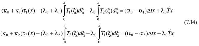
By differentiating, we find:

The next differentiation yields:

Because of the symmetry of the structure with respect to its mid-cross section, the interfacial thermal stresses are antisymmetric with respect to this cross section and can be sought in the form

where к is the thus far unknown parameter of the interfacial shearing stress. Introducing solutions (7.17) into equations (7.16) and requiring that the determinant of the obtained algebraic equations

is zero (otherwise the constants C, and C2 will also be zero), the following biquadratic equation for the parameter к can be obtained:

where the notations

are used. The 8 value characterizes the deviation of the parameter of the interfacial shearing stress in a trimaterial assembly from the magnitude of this parameter in a bimaterial assembly. This value changes from zero to one, when the axial compliance X0 of the inner (zero) component changes from zero to infinity, or, practically, to a large enough number exceeding the axial compliances of the two other components.
Biquadratic equation (7.19) results in the following formula for the parameter of the interfacial shearing stress:

When 6 = 0, then к = *Jkf+M. This result indicates that when the axial compliance of the inner component (such as a silicon chip) is considerably smaller than the axial compliance of the two other components (the substrate and the lid), the parameter к of the interfacial shearing stresses in the trimaterial assembly in question can be evaluated as the square root of the parameters squared of the interfacial shearing stresses of the upper and the lower bimaterial assemblies (the zero component is included in such a case in both the upper and the lower assemblies). If, in addition, the two outer components of the assembly are identical and characterized by the same interfacial stress parameter k„ then the interfacial stress parameter is k = k*yjl = .4142b. This result indicates that the parameter of the interfacial stress in a trimaterial assembly is always higher than in a bimaterial assembly. If all the three components in the trimaterial assembly are identical, then, with к = k = k2 = k*
and 8 =—, solution (7.20) yields
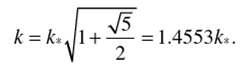
Thus, the interfacial stress parameter is always higher for a trimaterial assembly, than for a bimaterial one.
The induced force T{(x) acting in component #1 (substrate) can be sought in the form

The boundary conditions 71 (±/) = +T yield

In the mid-cross section of component #1 (x = 0), the sought solution (7.22) yields
 The second equation in (7.23) and equation (7.24) yield

For large enough kl values (long and stiff assemblies), these formulas can be simplified as

Introducing these formulas and the first formula in (7.23) into the sought solution (1.22), we obtain

Similarly, we find

These two solutions could be written as

These expressions satisfy the zero boundary conditions at the assembly ends and the conditions 7i.2(0) = 7i*2 in the mid-cross section (x = 0) of sufficiently long assemblies (kl —> ~). The interfacial shearing stresses can be determined by differentiation

At the assembly ends

For long assemblies with stiff interfaces (large kl values),
Peripheral Portions of the Design
The thermally induced forces acting in the cross sections of the assembly components of the peripheral portions of the design (Figure 7.4) can be evaluated using the same approach as the one used for the its midportion (Figure 7.3). The only difference is that in the peripheral portions of the design, the zero component and component #2 (lid) are made of the same material, and that there is just a single bonding material: the adhesive layer between component #1 (substrate) and the zero component, which is just part of the lid. The total force T (x) acting in component #1 (substrate) can be sought in the form (7.22), and the following three equations can be obtain for the constants C0,Cb and C<

The first equation determines the boundary condition for component #1 at its right end. The second equation is the boundary condition for this component at its left end. The third equation determines the force acting in the mid-cross section of component #1, assuming that the assembly is sufficiently long. Then, for large enough kl values, we find

and therefore

Similarly, we find

The two solutions can be combined as follows:

The interfacial shearing stresses can be determined by differentiation
 At the assembly ends

For long assemblies with stiff interfaces, these formulas yield

Clearly, when the force T is applied at the right end of a sufficiently long assembly, only this end will experience elevated stress caused by this force, while the remote end will not be affected at all.
The force T is “external” with respect to the midportion and the peripheral portions of the design, but is, as has been indicated, “internal,” as far as the design as a whole is concerned. This force can be found from the following condition of the compatibility of the displacements at the left boundary of the midportion of the design at its contact with the left peripheral portion:

The first term is the interfacial displacement at the right end of the peripheral portion of the design for component #1 (substrate), the second term is the interfacial displacement at the left end of the midportion of the design for the same component, the third term, evaluated using Hooke’s law, is the axial displacement of the portion of component #1 that is located between the design’s peripheral and the midportions; k0;, is the interfacial compliance of the zero component in the peripheral portion of the design (actually, of the lower part of the lid, whose thickness is the same as the thickness of the chip and the interfacial compliance of the bonding layer should be considered and included into this compliance); tc];, is the interfacial compliance of component #1 (substrate) at the peripheral portion of the design; K0m is the interfacial compliance of the chip (the interfacial compliances of the encapsulated solder joint layer and the thermal interface layer should be included into this compliance); Kim = Ki,, is the interfacial compliance of component #1 (substrate) at the midportion of the design;

is the interfacial shearing stress at the right end of the peripheral portion of the design; lp is half-the-length of the peripheral portion of the design; kp is the parameter of the interfacial shearing stresses at this portion; 7jp is the thermally induced force acting in component #1 (substrate) in the peripheral portion of the design;

is the interfacial shearing stress at the left end of the midportion of the design; l,„ is half-the-length of the midportion of the design; km is the parameter of the interfacial shearing stresses at this portion; Tm is the thermally induced force acting in component #1 (substrate) in the midportion of the design;

is the axial compliance of component #1 (substrate); £) is the effective Young’s modulus of the substrate material; v, is its Poisson’s ratio; 1ц is the substrate’s thickness; and Д is the length of the substrate’s portion between the chip and the lid. Equation (7.41) is the condition of the compatibility of the three displacements: the two interfacial displacements of the peripheral and the midportions of the design and the axial displacement of the gap portion of the substrate. The interfacial displacements are determined in accordance with the concept of the interfacial compliance, and the third one, in accordance with Hooke’s law.
Introducing expressions (7.42) and (7.43) into condition (7.41) and solving the obtained equation for the force T, the following formula for this force can be obtained:

One could certainly introduce this formula into equations (7.32) and (7.40) and obtain the analytical expressions that would consider the role of this force in a hidden fashion. We will, however, compute this force as part of the subsequent numerical examples. This will enable comparing the level of this force in comparison with the thermally induced forces acting in the cross sections of the assembly components.

