Numerical Examples
Design with an Organic Lid: Midportion of the Design
|
Structural Element |
«1 (Substrate) |
# 2 (Lid) |
|
#01 (TIL) |
#02 (ESJL) |
|
Thickness, mm |
1.0 |
1.0 |
0.5 |
0.05 |
0.1 |
|
Young’s modulus, kg/mm2 |
2300 |
800 |
13000 |
200 |
10000 |
|
Poisson’s ratio |
0.2S |
0.35 |
0.24 |
0.4 |
0.38 |
|
Shear modulus, kg/mm2 |
900 |
300 |
5200 |
70 |
3600 |
|
СТЕхЕб, 1/°C |
15.0 |
18.0 |
2.4 |
_ |
_ |
Half assembly length. /,„ =2.5mm; Change in temperature: At = 180°C; TIL = Thermal interface layer; ESJL = Encapsulated solder joint layer
• Determinant:

• Ratio:

Forces acting in mid-cross section of a long assembly:
• In the chip:

• In the substrate:

• In the lid:

Thus, the low expansion chip is in compression, while the substrate and the lid are in tension. The structure is in equilibrium so that the total force acting on it is zero. Interfacial compliances: [3]
• The lid:

Partial parameters of the interfacial shearing stress (for bimaterial assemblies):
 Parameter of the trimaterial assembly:

This parameter is small, because the zero component (high-modulus chip) is characterized by a very low axial compliance.
Parameter of the interfacial shearing stress:
Design with an Organic Lid: Peripheral Portion of the Design
Input data
|
Structural Element |
#1 (Substrate) |
£2 (Lid's Upper Part) |
0 (Lid's Lower Part) |
#01 (Adhesive Layer) |
|
Thickness, mm |
1.0 |
1.0 |
0.5 |
0.05 |
|
Young’s modulus, kg/mnd |
2300 |
800 |
800 |
200 |
|
Poisson’s ratio |
0.28 |
0.35 |
0.35 |
0.40 |
|
Shear modulus, kg/mnr |
900 |
300 |
300 |
70 |
|
СТЕхЕб, 1/deg.C |
15.0 |
18.0 |
18.0 |
- |
Half assembly length
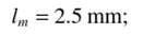
Change in temperature:

Calculated data
Axial compliances:
• Substrate:

• Lid’s upper part:

• Lid’s lower part:

• Determinant:

• Ratio:

Forces acting in mid-cross section of a long assembly: [4]
• In the lid:

Thus, the substrate is in compression, and the lid is in tension.
Interfacial compliances:
• The lid’s lower part (with the bonding layer):
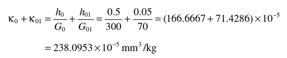
• The substrate:

• The lid’s upper part:

• Partial parameters of the interfacial shearing stress:

• Parameter of the trimaterial assembly:

This parameter is not small because all the assembly components are characterized by relatively high axial compliances.
• Parameter of the interfacial shearing stress:

• “External” force
The length of the substrate’s portion between the chip and the lid is Д = 7.5 mm Then, with

we obtain:

Interfacial shearing stresses:
• Maximum shearing stresses in the design’s midportion at the chip-substrate interface

• Maximum shearing stresses in the design midportion at the chip-lid interface

• Maximum shearing stresses in the design’s peripheral portion at the chip- substrate interface at its boundary with the midportion

• Maximum shearing stresses in the design’s peripheral portion at the chip- substrate interface and at its free boundary

• Maximum shearing stresses in the design peripheral portion at the chip-lid interface at its boundary with the midportion

• Maximum shearing stresses in the design’s peripheral portion at the chip- substrate interface at its free boundary

Design with a Copper Lid: Midportion of the Design
Input data
|
Structural Element |
#1 (Substrate) |
#2 (Lid) |
0 (Chip) |
«01 (TIL) |
#02 (ESJL) |
|
Thickness, mm |
l.O |
1.0 |
0.5 |
0.05 |
0.1 |
|
Young’s modulus, kg/mm2 |
2300 |
12200 |
13000 |
200 |
10000 |
|
Poisson’s ratio |
0.28 |
0.33 |
0.24 |
0.4 |
0.38 |
|
Shear modulus, kg/mm2 |
900 |
4586 |
5200 |
70 |
3600 |
|
СТЕхЕб. 1/°C |
15.0 |
16.5 |
2.4 |
- |
- |
Half assembly length, l,„ = 5.0mm Change in temperature: At = 180°C TIL =Thermal interface layer ESJL = Encapsulated solder joint layer
Calculated data
Axial compliances:
• Substrate:

• Lid:

• Chip:

• Determinant:

• Ratio:

Forces acting in mid-cross section of a long assembly: [7]
Thus, at low temperature condition, the low expansion chip is in compression, while the high expansion substrate and the lid are in tension. The structure is in equilibrium, so that the total force acting on it is zero. The thermally induced forces in the chip and in the lid of the design with a high-modulus lid are considerably higher than in a design with a low modulus lid: by the factor of about 2.2 for the chip and of about 5.6 for the lid. The induced force in the substrate went down considerably: there is only about 33% of the thermal force in it in the case of a low modulus lid. In effect, the forces in the chip and in the lid approximately equilibrate each other, while the substrate is understressed.
Interfacial compliances:
• The chip, with the TIL and the ESJL

• The substrate:

• The lid:

• Partial parameters of the interfacial shearing stress:

• Parameter of the trimaterial assembly:

• Parameter of the interfacial shearing stress:

Design with a Copper Lid: Peripheral Portions of the Design
Input data
|
Structural Element |
«1 (Substrate) |
«2 (Lid's Upper Part) |
|
«01 (Adhesive Layer) |
|
Thickness, mm |
1.0 |
1.0 |
0.5 |
0.05 |
|
Young’s modulus, kg/mm2 |
2300 |
12200 |
12200 |
200 |
|
Poisson’s ratio |
0.28 |
0.33 |
0.33 |
0.40 |
|
Shear modulus, kg/mm2 |
900 |
4586 |
4586 |
70 |
|
СТЕхЕб, l/deg.C |
15.0 |
16.5 |
16.5 |
- |
Half assembly length
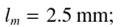 Change in temperature:

Calculated data
Axial compliances:
• Substrate:

• Lid’s upper part:

• Lid’s lower part:

• Determinant:

• Ratio:

Forces acting in mid-cross section of a long assembly:
• In the chip:

• In the substrate:

• In the lid:

Thus, the substrate is in compression, and the lid and the chip are in tension, as it is expected.
Interfacial compliances:
• The lid’s lower part (with the bonding layer):

• The substrate:

• The lid’s upper part:

• Partial parameters of the interfacial shearing stress:

• Parameter of the trimaterial assembly:

• Parameter of the interfacial shearing stress:

• “External” force
The length of the substrate’s portion between the chip and the lid is Д = 7.5 mm. Then, with

we obtain the following value for the “external” force:

Interfacial shearing stresses:
• Maximum shearing stresses in the design’s midportion at the chip-substrate interface

• Maximum shearing stresses in the design midportion at the chip-lid interface

• Maximum shearing stresses in the design’s peripheral portion at the chip- substrate interface at its boundary with the midportion

• Maximum shearing stresses in the design’s peripheral portion at the chip- substrate interface at its free boundary

• Maximum shearing stresses in the design peripheral portion at the chip-lid interface at its boundary with the midportion

• Maximum shearing stresses in the design’s peripheral portion at the chip- substrate interface at its free boundary

The computed data are summarized here:
|
Stresses, kg/mm2 |
With Plastic Lid |
With Copper Lid |
|
1 Maximum normal stress in the chip |
-14.1042 |
-30.5260 |
|
2 Maximum normal stress in the substrate in its midportion |
3.0588 |
0.6477 |
|
3 Maximum normal stress in the lid in its midportion |
3.9933 |
14.6153 |
|
4 Maximum shearing stresses in the design’s midportion at the chip-substrate interface |
+5.6468 |
+1.8366 |
|
5 Maximum shearing stresses in the design midportion at the chip-lid interface |
+3.9933 |
+10.9980 |
|
6 Maximum shearing stresses in the design’s peripheral portion at the chip-substrate interface at its boundary with the midportion |
-1.1558 |
-0.0962 |
|
7 Maximum shearing stresses in the design’s peripheral portion at the chip-substrate interface at its free boundary |
-0.7934 |
-0.5975 |
|
8 Maximum shearing stresses in the design peripheral portion at the chip-lid interface at its boundary with the midportion |
-2.4782 |
-1.0921 |
|
9 Maximum shearing stresses in the design’s peripheral portion at the chip-substrate interface at its free boundary |
0.5289 |
0.3984 |
The computed data indicate that the highest shearing stress occurs at the chip- bond interface and is significantly, by the factor of about 2.45, higher than the stress at the substrate-bond interface, but even the latter stress is about twice as high as the maximum shearing stress predicted on the basis of the bimaterial model. As to the normal stresses acting in the cross sections of the assembly components, the trimaterial model predicts that the highest stresses occur in the chip, the lowest in the substrate, and that the stresses in the bond are rather high, about 59% of the stresses in the chip. The bimaterial model, however, simply assumes that the normal stresses in the bond are zero. The normal stresses in the chip predicted on the basis of the bimaterial model are only about 78% of the stress predicted by the trimaterial model. The normal stresses in the substrate evaluated on the basis of the bimaterial model are almost twice as high as the trimaterial model predicts, but these stresses are low anyway: it is the state of stress in the chip and in the bonding layer, and the interfacial stress at the chip-bond interface that should be of concern to the device designer. It is concluded that while a simple bimaterial model can be successfully used for adhesively bonded assemblies, a trimaterial model should be employed for FC assemblies, especially when high-modulus solders are used. In addition, we conclude that the application of a copper lid, although might be desirable from the standpoint of thermal management of the design, leads to significantly higher maximum stresses, both the normal compressive stresses in the chip and the maximum interfacial shearing stresses; that the maximum normal stress in the chip is about twice as high in the design with a copper lid; that the maximum interfacial shearing stresses occur in the design midportion at the chip-substrate interface in the case of a plastic lid and at the chip-lid interface in the case of a copper lid; that the maximum interfacial shearing stress is also about twice as high in the design with a copper lid; and that the maximum shearing stresses are about a quarter of the maximum normal stresses. The developed model can be used in the analysis and design of the FC package of the type in question. The model can be particularly helpful when developing an FEA preprocessing simulation model. Future work should include FEA verifications of this model.
- [1] Calculated data Axial compliances: • Substrate: • Lid:
- [2] Chip:
- [3] The chip, with the thermal interface layer (TIL) and the encapsulated solderjoint layer (ESJL): • The substrate:
- [4] In the chip: • In the substrate:
- [5] This force is considerably larger than the thermally induced forces in the assemblycomponents. Stresses: Normal stresses in the assembly components: • Maximum normal (compressive) stress in the chip
- [6] Maximum normal (tensile) stress in the substrate in its midportion • Maximum normal (tensile) stress in the lid in its midportion
- [7] In the chip: • In the substrate: • In the lid:
- [8] This force is somewhat larger than the thermal forces acting in the lid and in thesubstrate, but the difference is not as significant as in the case of an organic lid.Stresses: Normal stresses in the assembly components: • Maximum normal stress in the chip
- [9] Maximum normal stress in the substrate in its midportion • Maximum normal stress in the lid in its midportion

