Numerical Example
Input data
|
Structural element |
#1 (Package) |
U2 (Substrate) |
0 (Bonding Material) |
|
Young’s modulus, kg/mm2 |
8775 |
2320 |
TBD |
|
Poisson’s ratio |
0.28 |
0.32 |
0.35 |
|
Shear modulus, kg/mm2 |
3428 |
879 |
TBD |
|
CTE. 1/°C |
6.5E-6 |
15.0E-6 |
X |
|
Thickness, mm |
2.0 |
1.5 |
0.05 |
|
Half package (assembly) length. / = 7.5 mm Measured force (within the elastic region) T = 0.325 kg/mm Corresponding (measured) displacement, = 2.6 x 10“5 mm Force at failure 7} = 36.0 kg/mm |
|||
Calculated data
Axial compliances:

Total interfacial compliance of the assembly
 Parameter of the interfacial shearing stress
 Shearing stress at the assembly end
 Stress at failure

Interfacial compliances of the assembly components

Interfacial compliance of the bonding layer
 Shear modulus of the bonding material

Tentative Young’s modulus
Possible Characterization of the Solder Material Properties
The developed model was also used to explain a paradoxical situation that was originally detected on the basis of finite element analysis (FEA) by Jorma Kivilahti and Tommi Reinikainen [48]: deep enough transverse grooves in the adherends (“pins”)
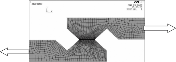
FIGURE 8.2 Transverse grooves in the adherends lead to lower and more uniformly distributed interfacial stresses.
(Figure 8.2) resulted in an appreciable reduction in, and to the more uniform distribution of, the interfacial shearing and peeling stresses. This phenomenon, important from the standpoint of testing solder materials, was explained based on analytical modeling by Suhir and Reinikainen [49, 50]. The model indicates that the observed phenomenon is due primarily to the increase in the interfacial compliance of the bonding structure: the grooves “convert” the adherend (“pin”) portions located between the inner portions of the grooves and the bonding (adhesive, solder) layer into parts of the bonding structure, thereby increasing the compliance of this structure with respect to the shearing load. This positive effect overwhelms, as far as the magnitude and the distribution of the interfacial stresses are concerned, the negative effect of the increased axial compliance of the loaded portions of the adherends (“pins”), because of the grooves.
The analytical predictions agree well with the FEA data, despite the FEA overestimation of the increase in the interfacial stresses in the proximity of the joint edges (as is known, FEA method, which is based on one of the numerical methods of the elasticity theory, leads to singular stresses at the edges of assemblies comprised of dissimilar materials).
The obtained information explains the physics of the phenomenon in question, and the developed analytical models can be used in the analysis and physical design of soldered lap shear joints. It is also concluded that analytical modeling is able not only to come up with relationships that clearly indicate “what affects what and what is responsible for what,” but, more importantly, can explain the physics of phenomena that neither the FEA modeling (“simulation”), nor even actual experimentation is able to. It is recommended that such tests are considered to obtain the mechanical properties of the solder materials for further analytical or FEA modeling.
CONCLUSION
elastic moduli of the bonding material if the interfacial displacement is also measured. In the author’s opinion, the suggested methodology, based on the concept of the interfacial compliance, could become a basis for a new effective experimental method for assessing the interfacial shearing strength and elastic moduli of the bonding material in electronics. The methodology can be used particularly in application to the recently suggested sintered silver bonding materials to evaluate their bonding strength from the measured force-at-failure and shear modulus from the measured shearing force and displacement.
References
- 1. M. Klein. B. Wiens, M. Hutter, H. Oppermann, R. Aschenbrenner, H. Reichl, “Behaviour of Platinum as UBM in Flip Chip Solder Joints,” Proceedings of the 50th ECTC. Nevada. May 2000.
- 2. R.H. Uang, K.C. Chen, S.W. Lu, H.T. Hu. S.H. Huang. “The Reliability Performance of Low Cost Bumping on Aluminum and Copper Wafer,” Proceedings of the 3rd Electronics Packaging Technology Conference (EPTC 2000), Singapore. Dec. 2000.
- 3. R.J. Coyle, P.P. Solan. A.J. Serafino, S.A. Gahr, “The Influence of Room Temperature Aging on Ball Shear Strength and Microstructure of Area Array Solder Balls,” Proceedings of the 50th ECTC. Nevada, May 2000.
- 4. K.M. Levis, A. Mawer, “Assembly and Solder Joint Reliability of Plastic Ball Grid Array with Lead-free versus Lead-Tin Interconnect,” Proceedings of the 50th ECTC, Nevada. May 2000.
- 5. Y. Tomita, Q. Wu, A. Maeda, S. Baba, N. Ueda, “Advanced Surface Plating on the Organic FC-BGA Package,” Proceedings of the 50th ECTC, Nevada. May 2000.
- 6. I.S. Kang, et al., “The Solder Joint and Runner Metal Reliability of Wafer-Level CSP (Omega-CSP),” Proceedings of the 50th ECTC. Nevada, May 2000.
- 7. S.-W.R. Lee, C.C. Yan, Z. Karim, X. Huang, “Assessment on the Effect of Electroless Nickel Plating on the Reliability of Solder Ball Attachment to the Bond Pads of PBGA Substrate,” Proceedings of the 50th ECTC. Nevada, May 2000.
- 8. C.K. Shin, J.Y. Huh, “Effect of Cu-containing Solders on the Critical IMC Thickness for the Shear Strength of BGA Solder Joints,” Proceedings of the 3rd Electronics Packaging Technology Conference (EPTC2000), Singapore, Dec. 2000.
- 9. S.Y. Jang, K.W. Paik, “Comparison of Electroplated Eutectic Sn/Bi and Pb/Sn Solder Bumps on Various UBM Systems,” Proceedings of the 50th ECTC, Nevada, May 2000.
- 10. S.J. Cho. J.Y. Kim. M.G. Park, I.S. Park. H.S. Chun. “Under Bump Metallurgies for a Wafer Level CSP with Eutectic Pb-Sn Solder Ball,” Proceedings of the 50th ECTC, Nevada, May 2000.
- 11. S.-W.R. Lee, K. Newman, L. Hu, “Thermal Fatigue Analysis of PBGA Solder Joints with the Consideration of Damage Evolution,” Packaging of Electronic and Photonic Devices. EEP. vol. 28. Florida, Nov. 2000.
- 12. D. Vogel, R. Kiihnert, M. Dost, B. Michel, “Determination of Packaging Material Properties Utilizing Image Correlation Techniques,” Journal of Electronic Packaging, vol. 124. 2002.
- 13. A. Schubert. R. Dudek, E. Auerswald, A. Gollhardt, B. Michel, H. Reichl, “Fatigue Life Models for SnAgCu and SnPb Solder Joints Evaluated by Experiments and Simulation,” 53rd ECTC. 2003.
- 14. R. Dudek, W. Faust, J. Vogel, B. Michel, “In-situ Solder Fatigue Studies Using a Thermal Lap Shear Test,” Proceedings of the International Conference on Electronics Packaging Technology, 2004.
- 15. R. Dudek, H. Walter, R. Doring, B. Michel, “Thermal Fatigue Modelling for SnAgCu and SnPb Solder Joints,” Proceedings of EuroSimE 2004, Brussels, Belgium, 2004.
- 16. A. Wymyslowski, et al., “Shearing tests for solder joints reliability assessment,” XXXI International Conference of 1MAPS Poland Chapter, Rzeszow-Krasiczyn, Poland, Sept. 2007.
- 17. J. Lau (ed.), Solder Joint Reliability: Theory and Applications, Van Nostrand Reinhold, 1990.
- 18. W. Engelmaier, “Reliability for Surface Mount Solder Joints: Physics and Statistics of Failure,” Proceedings of Surface Mount International, vol. 1, San Jose, California, Aug. 1992.
- 19. E. Suhir, “Stresses in Bi-Metal Thermostats,” ASME Journal of Applied Mechanics, vol. 53. No. 3, Sept. 1986.
- 20. E. Suhir, “Interfacial Stresses in Bi-Metal Thermostats,” ASME Journal of Applied Mechanics, vol. 56, No. 3, September 1989.
- 21. A.Y. Kuo, “Thermal Stress at the Edge of a Bi-Metallic Thermostat,” ASME Journal of Applied Mechanics, vol. 57, 1990.
- 22. C. Caswell, “Manufacturing and Reliability Challenges with QFN”, 1MAPS Conference, Atlantic City, New Jersey, June 2010.
- 23. E. Suhir, “Thermal Stress in a Bi-Material Assembly Adhesively Bonded at the Ends,” Journal of Applied Physics, vol. 89, No. 1, 2001.
- 24. E. Suhir, “Thermal Stress in an Adhesively Bonded Joint with a Low Modulus Adhesive Layer at the Ends,” Journal of Applied Physics, April 2003.
- 25. E. Suhir, “Interfacial Thermal Stresses in a Bi-Material Assembly with a Low-Yield- Stress Bonding Layer,” Modeling and Simulation in Materials Science and Engineering, vol. 14. 2006."
- 26. E. Suhir, “On a Paradoxical Situation Related to Bonded Joints: Could Stiffer Mid- Portions of a Compliant Attachment Result in Lower Thermal Stress?” Journal of Solid Mechanics and Materials Engineering (JSMME), vol. 3, No. 7, 2009.
- 27. E. Suhir, “Thermal Stress in a Bi-Material Assembly with a ‘Piecewise-Continuous’ Bonding Layer: Theorem of Three Axial Forces,” Journal of Physics D: Applied Physics, vol. 42, 2009.
- 28. E. Suhir, L. Bechou, B. Levrier, “Predicted Size of an Inelastic Zone in a Ball-Grid- Array Assembly,” ASME Journal of Applied Mechanics, vol. 80, March 2013.
- 29. E. Suhir, “Avoiding Low-Cycle Fatigue in Solder Material Using Inhomogeneous Column-Grid-Array (CGA) Design,” ChipScale Reviews, March-April 2016.
- 30. H. Schwarzbauer, “Method of Securing Electronic Components to a Substrate,” U.S Patent # 4 810 672. March 7, 1989.
- 31. H. Schwarzbauer, R. Kuhnert, “Novel Large Area Joining Technique for Improved Power Device Performance,” IEEE Transactions on Industry Applications, vol. 27, No. 1, Jan. 1991.
- 32. C. Mertens, R. Sittig, “Low Temperature Joining Technique for Improved Reliability,” International Conference on Integrated Power Electronic Systems, Bremen, Germany, 2002.
- 33. G. Bai, “Low-Temperature Sintering of Nanoscale Silver Paste for Semiconductor Device Interconnection,” Ph.D. dissertation, Virginia Polytechnic Institute and State University, Blacksburg, Virginia, Oct. 2005.
- 34. C. Gobi, P. Beckedahl, H. Braml, “Low Temperature Sinter Technology: Die Attachment for Automotive Power Electronic Applications,” Automotive Power Electronics, Paris, France, June 2006.
- 35. T. Wang, X. Chen, G.-Q. Lu, G.-Y. Lei, “Low-Temperature Sintering with Nano-Silver Paste in Die-Attached Interconnection,” Journal of Electronic Materials, vol. 36, No. 10. 1333-1340,2007.
- 36. N. Lubick, “Nanosilver Toxicity: Ions, Nanoparticles or Both?” Environmental Science and Technology, vol. 42, No. 23, 2008.
- 37. P.O. Quintero, T. Oberc, F. P. McCluskey, “High Temperature Die Attach by Transient Liquid Phase Sintering," HiTEC 2008. IMAPS, Albuquerque, New Mexico. May 2008.
- 38. M.H. Poech, M. Weiss, K. Gruber, “Chip Drop after Silver Sintering Process,” COMSOL Proceedings. Milan, Italy, 2009.
- 39. B. McPherson, et al., “Packaging of High-Temperature 50kW SiC Motor Drive Module for Hybrid Electric Vehicles,” Advanced Microelectronics, vol. 37, No. 1, Jan. 2010.
- 40. H.A. Mantooth, S. Ang, J.C. Baida, K. Okumura, T. Otsuka, “Packaging of High Temperature 50kW SiC Motor Drive Module for Hybrid-Electric Vehicles,” Advancing Microelectronics, vol. 37, No. 1, January 2010.
- 41. D. Wakuda, K.-S. Kim, K. Suganuma, “Ag Nanoparticle Paste Synthesis for Room Temperature Bonding,” IEEE CPMT Transactions, vol. 33, No. 1, March 2010.
- 42. T.G. Lei, J.N. Calata, G.-Q. Lu, X. Chen, S. Luo, “Low-Temperature Sintering of Nanoscale Silver Paste for Attaching Large-Area (>100 mm2) Chips,” IEEE CPMT Transactions, vol. 33, No. 1. March 2010.
- 43. M. Wrosch, A. Soriano, “Sintered Conductive Adhesives for High Temperature Packaging,” ECTC, 2010.
- 44. V. Manikam, K.Y. Cheong, “Die Attach Materials for High Temperature Applications: A Review,” CPMT Transactions, vol. 1, No. 4, April 2011.
- 45. C. Buttay, et al., “Die Attach of Power Devices Using Silver Sintering-Bonding Process Optimization and Characterization,” VDE Verlag GMBH, Berlin, Offenbach, Germany, Feb. 2012.
- 46. S. Kraft. A. Schletz, M. Maertz, “Reliability of Silver Sintering on DBC and DBA Substrates for Power Electronic Applications,” CIPS 2012, Nuremberg, Germany, Mar. 2012.
- 47. H. Jin, S. Kanagavel, W.-F. Chin, “Novel Conductive Paste Using Hybrid Silver Sintering Technology for High Reliability Power Semiconductor Packaging,” ECTC, 2014.
- 48. E. Suhir, T. Reinikainen, “On a Paradoxical Situation Related to Lap Shear Joints: Could Transverse Grooves in the Adherends Lead to Lower Interfacial Stresses?” Journal of Applied Physics D, vol. 41, 2008.
- 49. T. Reinikainen, E. Suhir, “Novel Shear Test Methodology for the Most Accurate Assessment of Solder Material Properties.” IEEE ECTC, 2009.
- 50. E. Suhir, T. Reinikainen, “Interfacial Stresess and a Lap Shear Joint (LSJ): The ‘Transverse Groove Effect’ (TGE),” Journal of Solid Mechanics and Materials Engineering (JSSME), vol. 3, No. 6, 2009.

